|
|
|
|
|
|
| |
|
|
| |
SMD REWORK: - Micro Assembly - FINEPLACER® Femto |
|
| |
|
|
| |
Micro Assembly: - |
|
|
|
|
| |
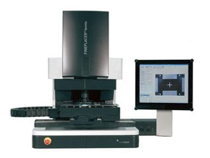
FINEPLACER® femto
Automated Sub-micron Die Bonder
The FINEPLACER® femto is a fully automated, sub-micron bonding platform for advanced packaging and optoelectronic applications.
This award winning system offers modular application architecture and can be flexibly equipped for a wide range of applications and processes. It is an ideal system for a production environment as well as for product and process development, accommodating the complete production workflow of inspection, characterization, packaging, final test and qualification.
FINEPLACER® femto has the best cost - performance ratio of its class in the market.
|
|
| |
| |
|
Highlights: - |
 |
|
- Sub-micron placement accuracy*
- Handles ultra small to very large components
- Fully-automated operation and assembly process
- Supports wafer/substrate sizes up to 12" *
- Supports bonding forces up to 500 N*
- Highly flexible platform architecture
- Small footprint and compact design
- Long-term stability
|
| |
|
|
| Features |
|
Benefits |
- Automated pattern recognition, alignment and bonding
- Overlay vision alignment system with fixed beam splitter in combination with automatic field extension and zoom
- Integrated Process Management (IPM)
- Adaptive process library
- Live process observation camera
- Virtually unlimited range of advanced bonding technologies
|
|
- Fully automated, user independent process
- Outstanding placement accuracy and instant operation without adjustments
- Synchronized control of all process related parameters: force, temperature, time, power,
- process environment, light and vision
- Fast and easy process development
- Immediate visual feedback reduces process development time
- ROI savings - one machine for all applications
|
| |
|
|
| Technologies |
|
Applications |
|
|
|
| |
|
|
| Technical Specifications |
|
|
| Placement accuracy*: |
|
± 0.5 µm |
| Field of view (min)1: |
|
0.27 mm x 0.2 mm |
| Field of view (max)1: |
|
3.2 mm x 2.4 mm |
| Component size (min): |
|
0.1 mm x 0.1 mm |
| Component size (max): |
|
100 mm x 100 mm |
| Theta fine travel: |
|
± 9° / 3.5 µrad |
| Z-travel / resolution: |
|
10 mm / 0.2 µm |
| Y-travel / resolution: |
|
150 mm / 0.1 µm |
| X-travel / resolution: |
|
450 mm / 0.1 µm |
| Working area: |
|
450 mm x 150 mm |
| Heating temperature1,2: |
|
400 °C |
| Bonding force range*: |
|
0.1 N - 500 N |
| |
|
|
| Modules & Options |
|
|
|
|
|
|
|
|
|
|
| |
|
|
|
|
|
|
|
