|
|
|
|
|
|
| |
|
|
| |
SMD REWORK: - Advanced Rework - FINEPLACER® micro hvr |
|
| |
|
|
| |
Advanced Rework: - |
|
|
|
|
| |
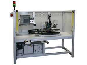
FINEPLACER® micro hvr
High Volume Rework Station
The FINEPLACER® micro hvr is a cost effective, fully-automated rework station, offering a high level of flexibility.
This award winning system is targeted for production environments where yield is crucial.
|
|
| |
| |
|
Highlights: - |
 |
|
- Components from 0.25 mm x 0.25 mm to 90 mm x 80 mm*
- Board sizes up to 350 mm x 260 mm*
- Closed loop force control
- Fully automated operation and soldering process
- Precise non-wearing xy planar table
- Traceability support with open data interface structure
- Flexible, cost effective performance
- Placement accuracy 10 µm @ 3 sigma
|
| |
|
|
| Features |
|
Benefits |
- Automated pattern recognition, alignment and soldering
- Overlay vision alignment system with fixed beam splitter
- Integrated Process Management (IPM)
- Adaptive process library
- Live process observation camera
|
|
- Hands-off component placement, user independent process operation
- Outstanding placement accuracy and instant operation without adjustments
- Provides high level of application flexibility
- Synchronized control of all process related parameters: force, temperature, time, flow, power, process environment, light and vision
- Immediate visual feedback reduces process development time
- Fast and easy process development
- Identical results on different machines allow central profile development,administration and distribution
|
| |
|
|
| Technologies |
|
Applications |
|
|
- Soldering of:
- BGA, µBGA/CSP, QFN, PoP, QFP, PGA,
- Small passives down to 0201
- RF shields, RF frames
- Connectors, sockets
- Sub assemblies, daughter boards
- Flipchip (C4)
- Single ball rework
|
| |
|
|
| Technical Specifications |
|
|
| Placement accuracy*: |
|
10 µm @ 3 sigma |
| Field of view (min)1: |
|
2.5 mm x 1.9 mm |
| Field of view (max)1: |
|
17.5 mm x 13 mm |
| Component size (min)1: |
|
0.25 mm x 0.25 mm |
| Component size (max)1: |
|
50 mm x 50 mm |
| Theta fine travel / resolution: |
|
± 4° / 1.0° |
| X-travel / resolution: |
|
380 mm / 0.64 µm |
| Y-travel / resolution: |
|
155 mm / 0.64 µm |
| Z-travel / resolution: |
|
8 mm / 0.8 µm |
| Top Heating: |
|
|
| Power: |
|
900 W |
| Temperature ramp rate: |
|
1 K/s - 50 K/s |
| Flow range: |
|
10 Nl/min - 70 Nl/min |
| Board Heating: |
|
|
| Power: |
|
1400 W |
| Heated area (max): |
|
330 mm x 170 mm |
| Flow range: |
|
48 Nl/min |
| |
|
|
| Modules & Options |
|
|
|
|
|
|
|
|
|
|
|
|
|
|
* depending on configuration/application
1 standard value, other values on request
2 optional module
|
|
| |
|
|
|
|
|
| |
|
|
|
|
